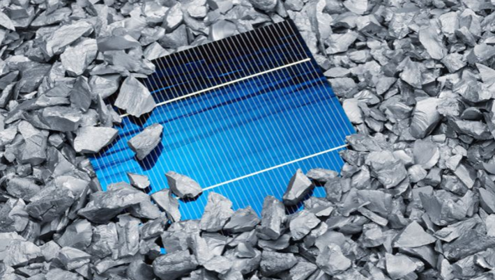
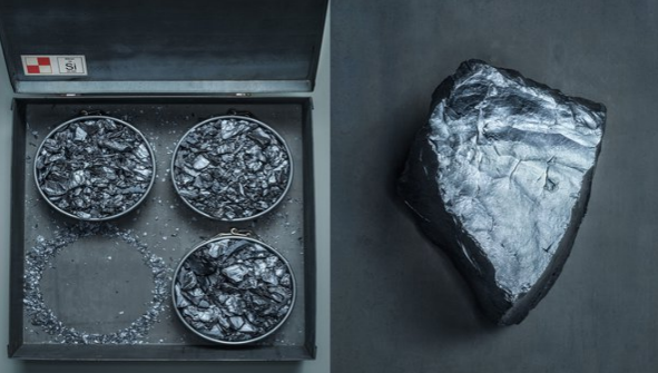
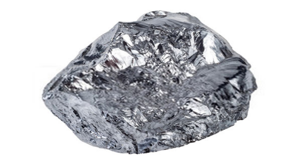
Pure silicon is expensive due to high production costs, environmental impacts, and increasing demand.
Methods of Silicon Purification
Silicon purification is an essential step in the semiconductor industry, ensuring the highest quality of silicon for electronic and photovoltaic applications. Various methods have been developed over the years to achieve ultra-pure silicon. Let’s delve into some of these key processes.

The Czochralski Process
The Czochralski Process is a widely used method to produce single-crystal silicon.
- Process Overview: A seed crystal of silicon is dipped into molten polycrystalline silicon. As the seed is slowly pulled up and rotated, a single-crystal silicon structure forms beneath it.
- Quality: Silicon crystals produced via this method are of high quality, typically with impurity levels below 1 part per billion (ppb).
- Efficiency: This method boasts an efficiency of approximately 85% in terms of raw silicon to final product conversion.
- Advantages: It produces large diameter wafers (typically up to 300mm) which are essential for modern semiconductor applications.
- Drawbacks: The primary drawback is the high cost, with prices reaching up to $20 per kilogram of finished silicon. The method also requires specialized equipment and high energy consumption, further driving up the price.
The Float-Zone Method
The Float-Zone Method is another technique primarily used for silicon purification, especially when ultra-high purity is essential.
- Process Overview: Silicon is refined by passing a polycrystalline silicon rod through a narrow zone of molten silicon. The impurities are driven off as the molten zone moves.
- Quality: It achieves even higher purity levels than the Czochralski process, often reaching impurity concentrations below 0.1 ppb.
- Efficiency: The efficiency stands at about 80%, slightly lower than the Czochralski process.
- Advantages: Exceptional purity makes it suitable for specific high-end applications like space-grade solar cells.
- Drawbacks: This method produces smaller diameter wafers, typically maxing out at 150mm. The process is also more expensive, with costs exceeding $25 per kilogram of the final product.
Chemical Vapor Deposition (CVD)
Chemical Vapor Deposition is a versatile process used not only for silicon purification but also for depositing various types of materials.
- Process Overview: Gaseous precursors react on a silicon wafer’s surface, depositing a layer of pure silicon.
- Quality: Purity levels are similar to the Czochralski method, with impurities typically below 1 ppb.
- Efficiency: CVD’s efficiency varies based on the specific process and equipment, but it generally falls between 75-90%.
- Advantages: CVD can be used to deposit various materials beyond just silicon, making it versatile. It also allows for precise thickness control.
- Drawbacks: The process is energy-intensive, with high costs reaching up to $30 per kilogram. Specialized precursor gases can also be expensive and pose storage challenges.
Each of these methods has its unique advantages, efficiencies, and cost implications, and their application largely depends on the specific requirements of the end product.

Factors Driving the Cost of Pure Silicon
Purifying silicon to the levels required for high-tech applications is no small feat. While the demand for ultra-pure silicon continues to rise, several factors influence its hefty price tag. Let’s examine these factors in detail.
Raw Material Costs
The foundational element for pure silicon is naturally occurring silicon dioxide, mainly sourced from quartz.
- Price of Quartz: As of recent data, high-grade quartz suitable for silicon production can cost anywhere from $50 to $100 per ton.
- Purity Requirements: The demand for high-purity quartz has escalated with the tech boom. Only a small fraction of mined quartz meets the purity standards, driving up the material’s price.
- Transportation: Given the weight and bulk of quartz, transporting it from mines to processing plants can add a significant cost, sometimes up to 10% of the material’s initial value.
Energy-intensive Production Processes
Silicon purification processes, as mentioned earlier, demand a great deal of energy, significantly influencing the final product’s cost.
- Power Consumption: For instance, the Czochralski process requires temperatures around 1,425°C. This means high energy bills, with electricity costs accounting for up to 30% of the total production cost.
- Carbon Footprint: High energy consumption not only means higher costs but also a larger carbon footprint, which can attract carbon taxes in certain jurisdictions.
Specialized Equipment and Facilities
The equipment used for silicon purification is intricate and often custom-made.
- Initial Investment: Setting up a facility equipped with the latest technology can demand an investment of over $1 billion.
- Maintenance Costs: The high precision required of this equipment means regular and often expensive maintenance, with yearly budgets often exceeding $10 million.
- Upgrade Cycles: With rapid technological advancements, equipment can become obsolete quickly, necessitating costly upgrades every 5 to 7 years.
Skilled Labor and Expertise Requirements
Expertise is crucial in the world of silicon purification.
- Training: Workers need rigorous training to handle the sophisticated equipment. Training programs can cost up to $5,000 per employee annually.
- Salaries: Given the niche expertise, salaries in the sector are higher than many other industries. A skilled technician’s average annual salary can range from $70,000 to $90,000.
- Research and Development: Constant innovation is key to maintaining a competitive edge in silicon production. R&D departments can have annual budgets exceeding $50 million, depending on the company’s size.
In conclusion, the journey of transforming natural quartz into ultra-pure silicon wafers is filled with hurdles, each contributing to the final product’s cost. As technological advancements surge forward, the importance and demand for pure silicon will only grow, making understanding these cost factors all the more essential.
Demand and Supply Dynamics
Balancing demand and supply is a continuous challenge in the silicon industry, with several factors at play. These dynamics not only affect the availability but also dictate the pricing of pure silicon.
The Growing Demand for Semiconductors
Silicon is the primary raw material for semiconductors, which are pivotal in almost every tech device we use today.
- Tech Proliferation: With the proliferation of smartphones, computers, and IoT devices, there’s an unprecedented demand for semiconductors. As of recent data, over 1 billion smartphones get sold annually, each containing a multitude of silicon-based chips.
- Emerging Technologies: Innovations like autonomous vehicles, AI, and augmented reality are further amplifying the demand. The semiconductor market has seen a steady annual growth rate of 5-7% over the past decade.
- Global Production Capacities: Despite increasing demand, semiconductor foundries can only increase their production capacity by about 3-5% annually, creating a supply-demand gap.
Limitations in Silicon Mining and Refinement
While silicon is the second most abundant element in the Earth’s crust, not all of it is suitable for semiconductor production.
- High-Purity Requirements: Only a minuscule fraction of mined silicon meets the rigorous purity requirements needed for semiconductors. Out of the millions of tons of silicon mined annually, only about 10% qualifies for further purification processes.
- Environmental Concerns: Silicon mining has environmental implications, which have led to stringent regulations in many countries. These regulations, while essential for the environment, can limit the rate at which silicon is mined. For instance, in regions like Europe, environmental regulations have increased the cost of mining by up to 15%.
- Refinement Challenges: As mentioned earlier, refining silicon to the required purity levels is energy-intensive and costly. The average cost of refining can range from $20 to $30 per kilogram, accounting for a significant portion of the final silicon price.
In conclusion, the tug of war between the soaring demand for semiconductors and the challenges in silicon mining and refinement results in volatile pricing and supply dynamics. As technology continues to evolve, understanding these dynamics becomes crucial for stakeholders in the semiconductor industry.

Environmental and Regulatory Considerations
The silicon industry, vital for technological advancements, also intersects with environmental and regulatory concerns. These considerations influence production processes, supply chains, and the industry’s overall sustainability.
Environmental Impact of Silicon Mining
Mining for silicon, primarily derived from quartz, has significant environmental repercussions.
- Land Degradation: Silicon mining, especially open-pit mining, can lead to habitat destruction and land degradation. For instance, a medium-sized silicon mine can disrupt up to 5 square kilometers of land annually.
- Water Consumption: The refinement processes for silicon are water-intensive. A single silicon refining facility can consume up to 2 million liters of water daily, straining local water resources.
- Chemical Pollution: The refining process uses chemicals like hydrochloric acid, which, if not managed properly, can pollute nearby water sources. For example, in some poorly managed facilities, chemical waste can increase local water pH levels by up to 15%.
- Carbon Emissions: As discussed, silicon refining is energy-intensive. A single facility can emit up to 100,000 tons of CO2 annually, contributing to global warming.
Regulatory Frameworks and Compliance Costs
Governments worldwide are instituting regulatory frameworks to mitigate the environmental impacts of silicon production.
- Emission Standards: Many countries have set strict emission standards for silicon producers. In places like California, plants that exceed a yearly emission of 50,000 tons of CO2 can face fines up to $100 per exceeded ton.
- Waste Management: Regulations mandate the proper disposal of chemical wastes. Non-compliance can result in penalties, with some jurisdictions levying fines up to $500,000 for significant violations.
- Rehabilitation Requirements: Some regions mandate that mining companies rehabilitate mined land. The cost of rehabilitating a single square kilometer can range from $1 million to $3 million.
- Water Use Restrictions: In water-scarce regions, there are stringent regulations on water usage. Overusing allocated water can result in penalties, sometimes costing companies up to 5% of their annual operational budget.
- Compliance Monitoring: Adhering to these regulations requires rigorous monitoring and reporting, further increasing operational costs. On average, a medium-sized silicon production facility can spend up to $2 million annually on compliance monitoring and reporting.
In a nutshell, while silicon plays a pivotal role in modern technology, its production comes with environmental costs. Regulatory frameworks aim to strike a balance between technological advancement and environmental sustainability, impacting the industry’s economics and operations. As the demand for silicon continues to rise, sustainable practices will become increasingly crucial.

Alternatives to Pure Silicon
tongwei thinks,As the demand for semiconductors continues its upward trajectory, the quest for alternatives to pure silicon intensifies. Silicon’s inherent limitations, combined with environmental and cost concerns, have paved the way for research into substitute materials and technologies.
Other Semiconductor Materials
Over the years, various materials have emerged as potential competitors to silicon in semiconductor applications.
- Germanium (Ge): Once the primary material for transistors, Germanium offers better electron mobility than silicon. However, it’s more expensive, with prices reaching up to $2,000 per kilogram, and has temperature sensitivity issues.
- Gallium Arsenide (GaAs): This compound offers faster electron movement and is often used in high-frequency applications. A significant downside is its cost, which can be up to 10 times that of silicon.
- Silicon Carbide (SiC): Suitable for high-power and high-temperature applications, Silicon Carbide is durable and can operate in harsher environments than pure silicon. The material’s cost ranges between $50 and $70 per kilogram, depending on quality.
- Graphene: A single layer of carbon atoms, Graphene boasts remarkable electrical conductivity and flexibility. The production cost, however, remains a challenge, with high-quality graphene sheets costing up to $100 per square centimeter.
Research on Cost-effective Alternatives
Innovation is vital in the search for cost-effective, scalable, and high-performance semiconductor alternatives to silicon.
- 2D Materials: Beyond graphene, there’s interest in other two-dimensional materials like molybdenum disulfide (MoS2). These materials have unique electronic properties, with production costs expected to decrease as techniques improve.
- Organic Semiconductors: Comprising carbon-based molecules, organic semiconductors offer the potential for flexible and low-cost electronics. Research is ongoing, with an average R&D budget in this domain reaching up to $10 million annually for leading firms.
- Quantum Dots: These nano-sized semiconductor particles have tunable electronic properties. While promising for various applications, large-scale production remains expensive, costing up to $10,000 per gram for high-quality quantum dots.
- Nano-tubes and Nano-wires: These materials have unique electrical, thermal, and mechanical properties. While promising, scalability and integration challenges persist. Research projects in this domain often have budgets ranging from $5 million to $7 million annually.
In conclusion, while silicon remains the dominant material in semiconductor technology, a combination of its inherent limitations and external challenges makes the search for alternatives both crucial and lucrative. The industry’s future might well hinge on how effectively and quickly these alternative materials transition from research labs to mass production.
