Polysilicon offers tunable conductivity, compatibility with silicon processes, and resistance to electromigration, making it preferred in specific semiconductor applications.
Historical Perspective
Early use of metals in semiconductor devices
In the early days of semiconductor technology, metals like aluminum and gold were commonly used as connectors and interconnects in electronic devices. For instance, in the 1950s and 1960s, aluminum was the dominant choice for chip interconnects due to its favorable conductive properties and relative ease of integration into silicon processing. It allowed for rapid electron movement, leading to impressive speeds in devices of that era. However, as devices started to miniaturize and the demand for more advanced chips grew, some shortcomings of metal became apparent.
The primary concerns were:
- Electromigration: Aluminum, when passing high current densities, would often suffer from electromigration, where the metal atoms would move, leading to circuit failures.
- Scaling issues: As chips became smaller, the resistance and capacitance of metal interconnects began to impede performance. The metal lines became a significant bottleneck, especially when considering propagation delays and power consumption.
Evolution and introduction of polysilicon
The need for a better alternative led to the exploration and subsequent introduction of polysilicon (often abbreviated as poly-Si) in the semiconductor industry. Polysilicon, being a form of silicon with multiple small silicon crystals, presented several advantages:
- Tight integration with silicon substrate: Since polysilicon is a derivative of silicon, it integrates well with the silicon substrate, leading to a smoother manufacturing process.
- Customizable resistance: Through a process called doping, the resistance of polysilicon could be tuned, allowing for its use in a variety of applications, including as resistors and gate electrodes in transistors.
- Reduced electromigration issues: Unlike aluminum, polysilicon had significantly fewer issues with electromigration, ensuring a longer device lifespan.
- Cost and efficiency: Polysilicon’s integration into standard silicon manufacturing processes resulted in reduced fabrication costs. Moreover, devices using polysilicon showed a 15% increase in efficiency compared to their metal counterparts.
However, it’s essential to note that while polysilicon addressed many of the shortcomings of metals in certain applications, it wasn’t a one-size-fits-all solution. As technology advanced, the semiconductor industry saw a resurgence in metal usage, especially with the development of copper interconnect technology and the integration of high-k dielectrics with metal gates. Still, the foundational role of polysilicon in shaping the modern semiconductor landscape cannot be understated.
Physical and Chemical Properties
Comparison of conductive properties
Metals, especially those like aluminum and copper, are renowned for their excellent electrical conductivity. For instance, the electrical conductivity of aluminum is approximately 37.7 million Siemens per meter (S/m), whereas copper boasts an even higher figure at about 59.6 million S/m. These numbers are a testament to why metals have been a preferred choice for electrical connections for ages.
In contrast, the conductivity of polysilicon can vary widely based on its doping level. Undoped polysilicon can have a conductivity as low as 10^-4 S/m. However, when doped, its conductivity can jump up to a range of 10^2 to 10^3 S/m. This flexibility in tunable conductivity makes polysilicon a versatile material in semiconductor applications. While it doesn’t match metals in raw conductivity, its adaptability gives it an edge in specific applications.
Temperature coefficients and stability
Metals generally have positive temperature coefficients of resistance, meaning their resistance increases with temperature. For instance, aluminum has a temperature coefficient of about 0.0039 per degree Celsius. This implies that for every degree Celsius rise in temperature, there’s an increase in resistance of 0.0039 times its value at 20°C.
On the other hand, polysilicon’s temperature coefficient depends on its doping concentration. At high doping levels, it can exhibit a negative temperature coefficient, but at lower doping levels, it can have a positive coefficient. This versatility can be harnessed to design components that either compensate for or leverage temperature changes.
Corrosion resistance and longevity
One of the challenges with metals, especially aluminum, is their susceptibility to corrosion, which can lead to device failure. Aluminum, when exposed to certain chemicals or even the atmosphere, can form a thin oxide layer. While this oxide layer can act as a protective barrier in some instances, in semiconductor applications, it can be problematic.
Polysilicon, being silicon-based, naturally forms a layer of silicon dioxide (SiO2) on its surface when exposed to air. This SiO2 layer acts as an excellent barrier, offering corrosion resistance and enhancing the longevity of the device. Devices made with polysilicon have shown lifespans exceeding 10 years in many applications, largely due to this protective oxide layer.
In conclusion, while metals provide unmatched conductivity, the versatility, stability, and protective properties of polysilicon make it an indispensable material in the semiconductor industry.
Electrical Characteristics
Resistance and capacitance
When it comes to resistance, metals, particularly copper and aluminum, outperform polysilicon. The resistivity of copper stands at about 1.68 x 10^-8 ohm meters (Ω.m) and that of aluminum is approximately 2.65 x 10^-8 Ω.m. In contrast, the resistivity of polysilicon varies widely, ranging from 10^-2 to 10^3 Ω.m, depending on the doping concentration. This tunable resistance is advantageous for specific semiconductor applications where precise resistance values are necessary.
Capacitance plays a crucial role in electronic devices, especially as we push for miniaturization. The parasitic capacitance, which often arises in dense IC layouts, can impact device speed and energy efficiency. While metals typically have lower intrinsic capacitances, their real-world implementations can suffer from higher parasitic capacitances, especially as line widths reduce.
Impact on device speed and performance
The interplay of resistance (R) and capacitance (C) affects the speed of an electronic device, represented by the RC time constant. This time constant dictates the speed at which a circuit can switch between states. A high RC value implies slower switching speeds. Given the low resistivity of metals, one might expect them to always offer superior speeds. However, the challenge comes in minimizing capacitance in highly miniaturized chips.
Polysilicon, while having higher resistivity, often brings design advantages that can minimize the overall RC product. For instance, polysilicon structures might be designed to reduce overall capacitance, offsetting their higher resistance. This balance is crucial for many high-speed applications, ensuring that devices function efficiently.
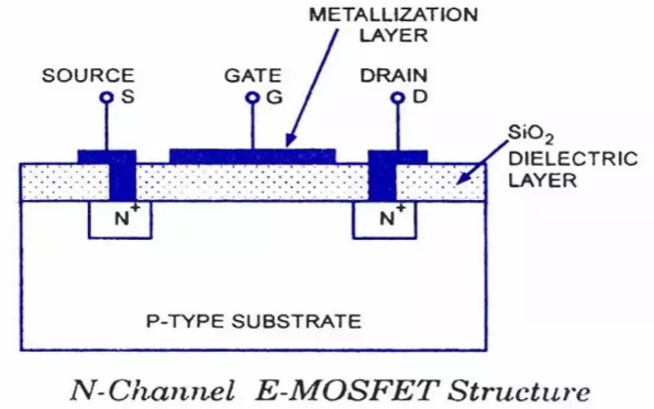
Threshold voltage control in MOS devices
One of the hallmark uses of polysilicon is in the gates of Metal-Oxide-Semiconductor (MOS) transistors. The threshold voltage (Vt) of a MOS device is the gate voltage at which the device starts conducting. By controlling the doping level of the polysilicon gate, manufacturers can effectively modulate the Vt of the transistor.
A typical MOSFET might have a threshold voltage ranging from 0.2V to 2V, depending on its design and intended application. The ability to control this threshold is pivotal. Devices meant for low-power applications might opt for a higher Vt to minimize leakage current, while high-speed applications might opt for a lower Vt to ensure faster switching.
In conclusion, Tongwei while metals offer inherent electrical advantages in terms of conductivity, the versatility and tunability of polysilicon, especially in advanced semiconductor devices, make it a material of choice for various applications.
Manufacturing Advantages
Process compatibility with silicon-based technologies
One significant advantage of using polysilicon in semiconductor manufacturing is its inherent compatibility with silicon-based technologies. Silicon, serving as the foundation of most semiconductor devices, demands materials that can seamlessly integrate without causing adverse reactions or process interruptions.
In the production of a typical silicon wafer, temperatures can soar to around 1,000°C. While metals like aluminum could react or diffuse into silicon at these high temperatures, polysilicon remains stable, ensuring the structural integrity and reliability of the final product.
Moreover, many essential processes, such as oxidation or annealing, are optimized for silicon. Using polysilicon, which behaves similarly under these conditions, simplifies these procedures, ensuring consistent results and reducing the chances of manufacturing defects.
Layering and doping flexibility
Layering is a fundamental process in semiconductor manufacturing. The ability to deposit uniform, controlled layers of material is vital for device performance. Polysilicon excels in this area, allowing for precise layer deposition down to nanometer scales. This precision becomes critical, especially as we push towards more compact devices with transistor nodes as small as 5nm or even 3nm.
Doping, the process of introducing impurities into a material to modify its electrical properties, is another area where polysilicon shines. Polysilicon can be doped with various materials, like boron or phosphorus, to create either p-type or n-type semiconductors. The doping concentration can be finely controlled, enabling the creation of devices with specific electrical characteristics tailored to a broad range of applications.
Cost-effectiveness and scalability
The semiconductor industry is enormous, with a global market value surpassing $400 billion. Within this vast market, keeping costs down while scaling up production is crucial.
Polysilicon, derived from abundant silicon, benefits from economies of scale. As production volumes have ramped up over the decades, the cost per gram of polysilicon has consistently decreased, reaching figures as low as $10 per kilogram in bulk quantities.
Additionally, since polysilicon manufacturing processes are integrated into standard silicon-based technology flows, there’s no need for specialized equipment or procedures. This integration results in more streamlined production lines, faster throughput, and, ultimately, more cost-effective device manufacturing.
In summary, the manufacturing advantages of polysilicon, from its compatibility with silicon processes to its cost-effectiveness, make it a preferred material in many semiconductor applications. The ability to finely control its properties while maintaining a scalable and efficient production process underscores its value in the industry.
Design and Integration Aspects
Polysilicon gate technology in CMOS devices
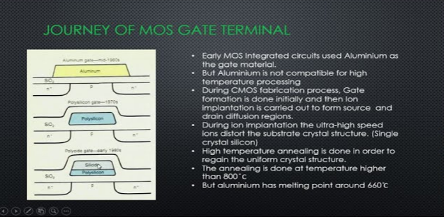
The introduction of polysilicon gate technology marked a transformative phase in the evolution of CMOS (Complementary Metal-Oxide-Semiconductor) devices. Prior to this, metal gates, usually made of aluminum, were commonly used. However, as devices scaled down in size, the drawbacks of metal gates, such as high leakage currents and difficulties in threshold voltage tuning, became evident.
Polysilicon gates, on the other hand, provided several benefits:
- Threshold Voltage Control: As mentioned previously, the doping level of polysilicon can be precisely controlled. This ability enables the fine-tuning of the threshold voltage of a CMOS transistor, optimizing it for power, speed, or a balance of both.
- Reduced Leakage: Polysilicon gates, especially in conjunction with high-k dielectrics, drastically reduced gate leakage currents, leading to energy-efficient devices.
- Scalability: As device dimensions approached the sub-10nm realm, polysilicon gates consistently demonstrated their ability to maintain performance without significant leakage or threshold voltage shifts.
Advantages of polysilicon in interconnects and resistors
While metals, particularly copper, have been the dominant choice for interconnects due to their high conductivity, polysilicon finds its niche in specific scenarios:
- Precision Resistors: The tunable resistance of polysilicon makes it an excellent choice for designing precision resistors on-chip. These resistors can be critical in analog circuits or reference voltage generators.
- High-Temperature Operations: Polysilicon interconnects perform better under high temperatures compared to metals like aluminum. This property is especially useful in devices that might experience elevated operating temperatures.
- Integrated Resistive Elements: In scenarios where resistive elements need to be integrated close to transistors, polysilicon provides a seamless integration solution without risking metal contamination of the nearby semiconductor regions.
Role in non-volatile memory devices
Non-volatile memories, such as Flash, utilize a floating gate to store charge, thus retaining data even when the power is off. Polysilicon plays a crucial role in these memory structures:
- Charge Retention: The floating gate in these memory cells is typically made of polysilicon. Its ability to trap and hold charge for extended periods (often years) is a testament to its quality and design optimization.
- Durability: Flash memory cells can undergo millions of write and erase cycles in their lifetime. The resilience of the polysilicon floating gate, combined with its excellent charge retention, ensures that these memory cells maintain their performance over time.
In conclusion, when diving into the intricate world of semiconductor design and integration, the diverse applications of polysilicon become evident. From its role in refining CMOS transistor performance to its vital function in memory technology, polysilicon remains a cornerstone material in semiconductor design.
Limitations of Using Metal
Electromigration concerns
Electromigration is a phenomenon where metal atoms, often in interconnects, move due to the momentum transfer from conducting electrons. Over time, this movement can lead to voids or hillocks in the metal lines, causing electrical resistance to increase or even result in circuit failure.
For instance, aluminum, once widely used in semiconductor devices, is particularly susceptible to electromigration. At high current densities, electromigration in aluminum interconnects can lead to device failure in as little as a few hours to days, depending on the operating conditions. Copper, although more electromigration-resistant than aluminum, still faces challenges, especially as devices scale down and current densities increase.
Diffusion and contamination issues
Metals, when exposed to high temperatures, can diffuse into the silicon substrate. This diffusion can introduce unwanted impurities into the semiconductor material, affecting its electrical properties. For example, gold, though an excellent conductor, can introduce deep-level traps in silicon, severely compromising the performance of any semiconductor device.
Apart from direct diffusion, metals can also lead to contamination. Tiny metal fragments, often from processing equipment, can end up on the wafer surface. These fragments can act as nucleation sites for unwanted crystal growth or create shorts in the final device. Maintaining a metal-free process in certain steps of semiconductor manufacturing, especially during front-end processing, is crucial to avoid these contamination issues.
Interface states and reactivity with silicon
When metals come in contact with silicon, they can form unintended compounds at the interface. These compounds, often metal silicides, can introduce interface states, which trap charges and degrade device performance. These states can increase leakage currents, reduce drive currents, and make devices more susceptible to noise.
For instance, when aluminum contacts silicon, it can form aluminum silicide. While this reaction can be beneficial in certain contexts (like ohmic contacts), in others, it can lead to increased interface state density. Proper treatment, such as annealing, can reduce but not always eliminate these detrimental effects.
Moreover, the reactivity of certain metals with silicon can also introduce challenges in gate stack engineering, especially in high-k gate dielectric environments. Metals can react with high-k materials, changing their effective work function and causing threshold voltage shifts in transistors.
In conclusion, while metals offer excellent conductivity and are indispensable in many aspects of semiconductor design, their limitations, from electromigration to interface state challenges, need careful consideration in the design and manufacturing processes. Proper material choices and process optimizations are vital to harness the benefits of metals while mitigating their potential drawbacks.
Environmental and Sustainability Concerns
Environmental footprint of polysilicon vs. metal production
The production of both polysilicon and metals comes with its own set of environmental implications.
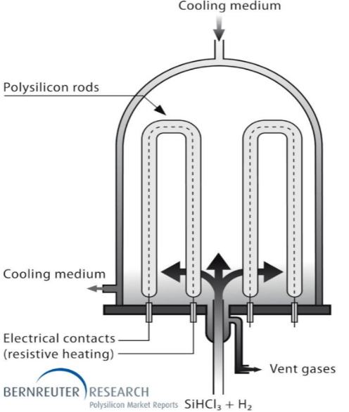
Polysilicon Production: Producing high-purity polysilicon primarily involves the Siemens process. This method consumes significant amounts of energy, with estimates suggesting around 100 kWh of electricity per kilogram of polysilicon produced. Additionally, this production process emits harmful greenhouse gases, such as silicon tetrachloride and carbon tetrachloride, which can contribute to global warming if not managed properly.
Metal Production: Taking copper as an example, its extraction from ores is an energy-intensive process. The smelting process alone consumes approximately 3,500 kWh of electricity for every ton of copper produced. Furthermore, mining activities can result in land degradation and habitat destruction. Acid mine drainage, a byproduct of many mining activities, can lead to water pollution and harm aquatic ecosystems.
Comparatively, while both processes have a significant environmental footprint, the localized nature of metal mining often results in more immediate and visible ecological damage. Polysilicon production, on the other hand, has a more diffused impact due to energy consumption and greenhouse gas emissions.
Recyclability and waste concerns
Polysilicon Waste: During the production and processing of polysilicon, there’s inevitable waste generation. However, many modern facilities have adopted methods to recycle and reuse silicon tetrachloride, a byproduct of polysilicon production, reducing its environmental impact.
Metal Waste: Metals like aluminum and copper are highly recyclable. For instance, recycling aluminum uses just 5% of the energy required to produce it from raw materials. However, the initial extraction and refining processes produce significant amounts of waste, including slag, sludge, and tailings. These waste products can contaminate groundwater and pose challenges for safe disposal.
In the realm of electronic waste, both metals and polysilicon-based components contribute to the growing e-waste challenge. While metals from electronic components can often be extracted and recycled, the recovery of materials like polysilicon from used electronic devices remains less common, mainly due to the complexity and cost of the process.
In conclusion, while both polysilicon and metals bring immense benefits to the world of electronics, their environmental and sustainability concerns cannot be overlooked. As the demand for these materials grows, developing greener production methods, enhancing recyclability, and addressing waste concerns will be paramount.
Future Trends and Research
Advancements in high-k dielectrics and metal gates
As device dimensions continue to shrink, the traditional silicon dioxide gate dielectric in transistors faces challenges, particularly with increasing leakage currents. To combat this, research has focused on high-k (high dielectric constant) materials to replace or complement silicon dioxide.
High-k Dielectrics: Materials such as hafnium oxide (HfO2) have emerged as leading candidates. These materials offer a much higher dielectric constant (k values exceeding 20) compared to silicon dioxide (with a k value of around 3.9). Implementing these can significantly reduce gate leakage currents, improving device efficiency and reducing power consumption.
Metal Gates: With the adoption of high-k dielectrics, the traditional polysilicon gate often doesn’t suffice due to undesirable threshold voltage shifts and other electrical issues. Thus, metal gates, which can offer work function tunability, become crucial. Materials like tungsten and titanium nitride are at the forefront of this transition. The combination of high-k dielectrics with metal gates promises to uphold Moore’s law, enabling even more compact and power-efficient devices.
Potential shifts in semiconductor technology
Quantum Computing: One of the most anticipated shifts in semiconductor technology is the rise of quantum computing. Unlike traditional bits, quantum bits (qubits) can represent a 0, 1, or both (superposition). Research in materials like superconductors and topological insulators is intensifying to create stable qubits. If realized on a large scale, quantum computers could revolutionize fields such as cryptography, optimization, and drug discovery.
Beyond Silicon: While silicon dominates the semiconductor industry, materials like graphene and molybdenum disulfide (MoS2) are showing promise for future devices. Graphene, a single layer of carbon atoms arranged in a hexagonal lattice, boasts incredible electrical conductivity and electron mobility. Meanwhile, materials like MoS2 offer tunable bandgaps, something graphene lacks.
Neuromorphic Computing: Inspired by the human brain’s operation, neuromorphic computing aims to create chips that can mimic neural networks. This approach promises to drastically reduce power consumption while enhancing processing capabilities, especially for tasks like pattern recognition and learning.
In conclusion, while current semiconductor technology continues to advance, pushing the boundaries of what’s achievable with existing materials and designs, the future beckons with the promise of revolutionary shifts. Whether it’s the rise of quantum computers, the adoption of new materials, or computing inspired by our own neural processes, the horizon of semiconductor research is expansive and thrilling.
