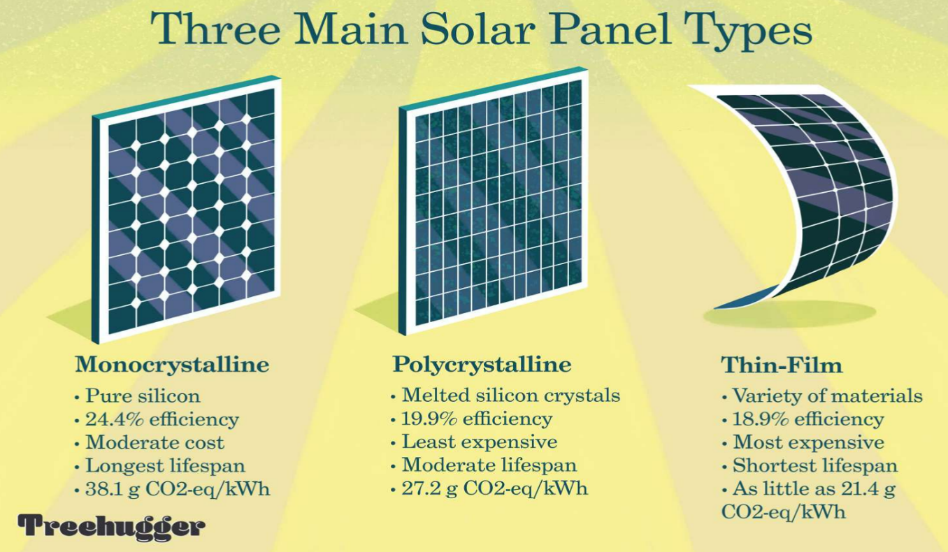
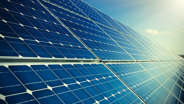
Monocrystalline silicon wafers are the most efficient type.
Types of Crystalline Silicon Wafers
Crystalline silicon wafers are pivotal components used predominantly in the manufacturing of photovoltaic cells and semiconductor devices. They play a critical role in transforming sunlight into electricity efficiently. These wafers are divided mainly into three types, which vary based on crystal structure, efficiency, production methods, and cost.

Monocrystalline Silicon Wafers
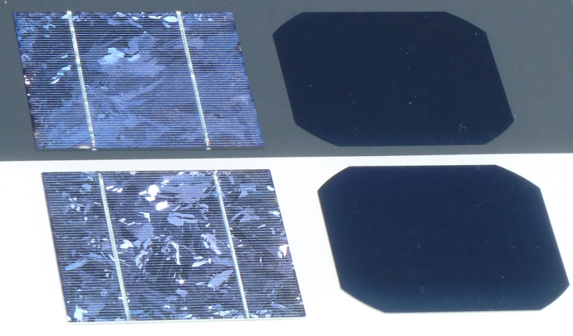
Monocrystalline silicon wafers are developed from a single crystal structure, enabling electrons to move freely, which subsequently boosts the efficiency of solar cells made from them. They are recognizable by their dark black color and rounded edges.
- Specifications and Parameters
- Efficiency: Approximately 20% – 25%
- Lifespan: Generally, around 25 – 30 years
- Size: Commonly found in 156 mm x 156 mm dimensions
- Cost: Typically higher, around $20 per square foot due to the intricate manufacturing process
- Advantages and Disadvantages
- Advantages: Higher efficiency and longer lifespan make them suitable for space-constrained installations
- Disadvantages: Higher production cost and waste of silicon during the manufacturing process
- Applications and Usage
- Primarily used in high-quality solar panels and sophisticated electronic devices due to its high efficiency and purity
Polycrystalline Silicon Wafers
Polycrystalline silicon wafers, distinguished by their blue color and square shape, are manufactured by melting multiple silicon fragments together. This results in several crystal structures in each wafer.
- Specifications and Parameters
- Efficiency: Ranges between 15% – 20%
- Lifespan: Roughly 23 – 27 years
- Size: Typically available in 156 mm x 156 mm dimensions
- Cost: More budget-friendly, approximately $15 per square foot, due to a less complicated manufacturing process
- Advantages and Disadvantages
- Advantages: Lower cost and less silicon waste during production
- Disadvantages: Lower efficiency due to the presence of multiple crystal structures causing more obstructions to electron movement
- Applications and Usage
- Ideal for large-scale installations where space is not a constraint, like solar farms, due to their lower cost and adequate efficiency levels
Amorphous Silicon Wafers
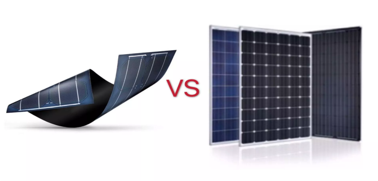
Amorphous silicon wafers are non-crystalline and have a randomized atomic arrangement. They are known for their flexibility and are typically utilized for thin-film solar cells.
- Specifications and Parameters
- Efficiency: Approximately 10% – 12%
- Lifespan: Around 15 – 20 years
- Size: Variable, as they are primarily used for thin-film applications
- Cost: Generally lower, around $10 per square foot, owing to the simpler production process
- Advantages and Disadvantages
- Advantages: Flexible, lightweight, and can be used on unconventional surfaces like rolled roofing
- Disadvantages: Lower efficiency and shorter lifespan compared to crystalline counterparts
- Applications and Usage
- Suited for applications like portable solar panels and calculators where flexibility and lightweight attributes are crucial, and high efficiency is not the priority.
Summary
In conclusion, each type of crystalline silicon wafer offers unique advantages, disadvantages, specifications, and applications, addressing different needs and preferences in the renewable energy and electronics sectors. The selection of the appropriate type primarily depends on specific requirements like efficiency, cost, size, lifespan, and application.
Manufacturing Processes
The manufacturing processes of silicon wafers are crucial, as they have a direct impact on the efficiency, quality, and cost of the final product. These processes essentially determine the crystal structure and purity of the silicon wafers, which are pivotal for applications in solar cells and semiconductor devices.
Czochralski Process (CZ)
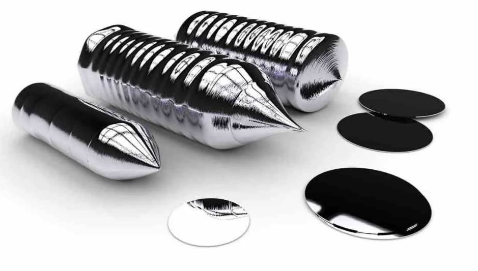
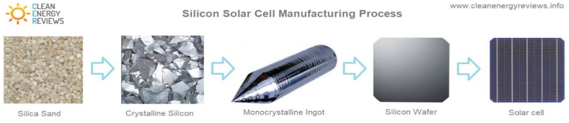
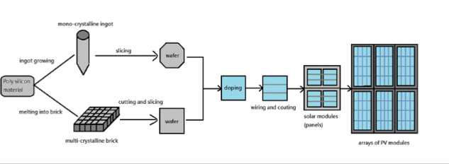
The Czochralski Process is a widely used method for producing monocrystalline silicon wafers. It involves dipping a seed crystal into molten silicon and slowly pulling it up, allowing a single crystal to form around it.
- Specifications and Parameters
- Time: It usually takes around 18 – 36 hours to complete one cycle.
- Cost: It is relatively expensive due to the high energy consumption, approximately $25 per square foot.
- Quality: It produces high-purity and defect-free crystals, crucial for high-efficiency applications.
- Advantages and Disadvantages
- Advantages: High purity and quality of the silicon wafers, suitable for sophisticated electronic devices and high-efficiency solar cells.
- Disadvantages: High cost and significant material wastage, as the cylindrical crystal has to be trimmed to form wafers, leading to loss of material.
- Applications and Usage
- Predominantly used for manufacturing high-quality and efficient monocrystalline silicon wafers for applications like advanced solar cells and integrated circuits.
Float Zone Process (FZ)
The Float Zone Process is another technique utilized for the production of high-purity silicon wafers, and it is especially useful for manufacturing semiconductor devices.
- Specifications and Parameters
- Time: The process is time-intensive, often requiring over 24 hours per cycle.
- Cost: The high energy requirement makes it an expensive method, with prices around $30 per square foot.
- Quality: It yields extremely high-purity silicon, ideal for advanced semiconductor applications.
- Advantages and Disadvantages
- Advantages: Superior purity and quality of silicon without the need for a crucible, beneficial for creating sensitive semiconductor devices.
- Disadvantages: High cost, complexity, and limited to smaller diameter wafers due to the inherent instability of the process.
- Applications and Usage
- Ideal for producing silicon wafers for advanced semiconductor devices where extreme purity is paramount, such as in scientific research and specialized electronic components.
Casting Process
The Casting Process, also known as the multicrystalline or polycrystalline process, involves pouring molten silicon into a square mold, allowing it to solidify into a block which is then sawed into individual wafers.
- Specifications and Parameters
- Time: It requires less time compared to other processes, typically around 12 – 24 hours per cycle.
- Cost: It is more economical, costing approximately $15 per square foot, making it suitable for large-scale production.
- Quality: It produces wafers with multiple crystal structures, resulting in lower efficiency compared to monocrystalline wafers.
- Advantages and Disadvantages
- Advantages: Lower cost, simpler process, and less material wastage compared to the Czochralski process.
- Disadvantages: Lower efficiency and quality due to the presence of grain boundaries that impede electron movement.
- Applications and Usage
- Primarily used for manufacturing polycrystalline silicon wafers for applications where cost is a significant factor, such as in commercial solar panels and large-scale solar farms.
Summary
Each manufacturing process is tailored to meet specific requirements related to cost, efficiency, quality, and applications of the silicon wafers. The selection between the different processes is primarily governed by the intended application, budget constraints, and desired quality of the final product.
Evaluation of Efficiency
Efficiency in silicon wafers is crucial as it determines the performance of the end products such as solar cells and semiconductor devices. It is imperative to understand, measure, and optimize the efficiency of silicon wafers to enhance the overall functionality and cost-effectiveness of the final products.
Definition of Efficiency in Silicon Wafers
Efficiency in silicon wafers, particularly in the context of solar cells, refers to the proportion of sunlight’s energy that can be converted into usable electrical energy. It is a critical parameter and is usually expressed as a percentage, representing the energy conversion efficiency of the silicon wafer.
- How It’s Calculated
- Efficiency is computed as the output electrical power divided by the input solar power, typically measured under standard test conditions.
- Importance of Efficiency
- High efficiency means more power can be generated from a smaller area, which is crucial for applications with space constraints such as rooftop solar installations.
Measurement of Efficiency
Measuring the efficiency of silicon wafers accurately is crucial for optimizing performance. This involves assessing the electrical output under controlled conditions to ensure reliability of the results.
- Methods of Measurement
- The most common method involves illuminating the wafer with a known quantity of light energy and measuring the electrical energy output.
- Use of specialized equipment like solar simulators to replicate standard test conditions is crucial for accurate measurement.
- Standard Test Conditions
- Standard conditions typically involve a temperature of 25°C and an irradiance of 1000W/m² with the light spectrum of AM 1.5.
Factors Influencing Efficiency
Various factors influence the efficiency of silicon wafers, such as the purity of the silicon, the manufacturing process, and the presence of defects in the crystal structure.
- Material Purity
- Higher purity of silicon generally results in higher efficiency as impurities can impede the flow of electrons and create energy loss.
- Crystal Structure
- Monocrystalline structures tend to have higher efficiency compared to polycrystalline and amorphous structures due to fewer obstacles to electron movement.
- Manufacturing Process
- The choice of manufacturing process can impact the efficiency due to variations in material quality, crystal structure, and the presence of defects.
- Temperature
- Efficiency can also be affected by temperature variations, with higher temperatures generally leading to decreased efficiency due to increased resistance.
Summary
The efficiency of silicon wafers is a pivotal aspect, influencing the performance and applications of the final products. Proper evaluation, which includes precise definition, accurate measurement under standardized conditions, and thorough understanding of the influencing factors, is essential for the optimization and advancement of silicon-based technologies. The relentless pursuit of higher efficiency levels will continue to drive innovations in materials, manufacturing processes, and applications in the field of silicon wafers.
Comparison of Efficiency between Different Types
Tongwei thinks,Comparing the efficiency between different types of silicon wafers is crucial for determining their suitability for specific applications. The choice between monocrystalline, polycrystalline, and amorphous silicon wafers will depend on various factors, including efficiency requirements, budget constraints, and specific application needs.
Efficiency of Monocrystalline Silicon Wafers
Monocrystalline silicon wafers, composed of single crystal silicon, usually have the highest efficiency among the three types due to their uniform crystal structure allowing unimpeded electron movement.
- Performance and Specifications
- Efficiency: These wafers typically have an efficiency range of 15% to 22%.
- Cost: They are generally more expensive due to the complex manufacturing process, costing approximately $25 per square foot.
- Application: They are ideal for applications where high efficiency is crucial, such as space-constrained rooftop solar installations and high-performance electronic devices.
- Advantages and Disadvantages
- Advantages: High efficiency, long lifespan, and optimal performance in low-light conditions.
- Disadvantages: Higher cost and more waste produced during the manufacturing process.
Efficiency of Polycrystalline Silicon Wafers
Polycrystalline silicon wafers are composed of multiple crystal structures, leading to lower efficiency due to the presence of grain boundaries that obstruct electron movement.
- Performance and Specifications
- Efficiency: Typically, they have an efficiency range of 13% to 16%.
- Cost: More budget-friendly, costing around $15 per square foot due to a simpler manufacturing process.
- Application: Suitable for large-scale solar installations where space is not a constraint and cost-effectiveness is prioritized.
- Advantages and Disadvantages
- Advantages: Lower cost and less waste produced during manufacturing.
- Disadvantages: Lower efficiency and shorter lifespan compared to monocrystalline wafers.
Efficiency of Amorphous Silicon Wafers
Amorphous silicon wafers lack a defined crystal structure, resulting in the lowest efficiency among the three types due to extensive electron recombination.
- Performance and Specifications
- Efficiency: Their efficiency generally falls below 10%.
- Cost: They are the most economical, costing around $10 per square foot.
- Application: Mainly used in applications like calculators and other small electronic devices where high efficiency is not a priority.
- Advantages and Disadvantages
- Advantages: Very low cost, flexibility, and lightweight.
- Disadvantages: Significantly lower efficiency and stability over time.
Summary
The comparative analysis of efficiency between different types of silicon wafers is crucial for their application in the renewable energy and electronics sectors. Monocrystalline wafers are suitable for applications requiring high efficiency, regardless of the cost. Polycrystalline wafers are optimal for large-scale applications where budget is a significant factor. Lastly, amorphous silicon wafers, with their flexibility and low cost, find usage in smaller, less efficiency-dependent applications.
Applications
Silicon wafers have diverse applications due to their varied types and inherent properties. The use of monocrystalline, polycrystalline, and amorphous silicon wafers is widespread, each fitting specific needs and industry demands based on their characteristics like efficiency, cost, and flexibility.
Applications of Monocrystalline Silicon Wafers
Monocrystalline silicon wafers, known for their high efficiency and long lifespan, are prevalently used in premium solar panels and sophisticated electronic devices.
- Solar Panels
- Their high efficiency makes them the preferred choice for compact, space-constrained solar installations, such as residential rooftop panels, where maximizing power output is essential.
- Electronics
- Used in high-performance electronic devices like smartphones and computers due to their superior electrical characteristics and reliability.
- Space Technology
- Frequently employed in space applications where high efficiency and reliability under extreme conditions are vital.
Applications of Polycrystalline Silicon Wafers
Polycrystalline silicon wafers, balancing cost and efficiency, are mainly used in sectors where space is ample, and budget is a crucial factor.
- Large-Scale Solar Farms
- Due to their cost-effectiveness, they are typically used in expansive solar farms where space availability mitigates their lower efficiency.
- Low-Cost Electronics
- They find usage in economical electronic devices where high efficiency is not paramount, and cost savings are prioritized.
Applications of Amorphous Silicon Wafers
Amorphous silicon wafers, being flexible and economical, are applied predominantly in small, portable electronic devices and thin-film technology.
- Calculators and Watches
- Their flexibility and low cost make them suitable for small devices like calculators and watches where high efficiency is not required.
- Thin-Film Solar Panels
- Used in lightweight, flexible solar panels, which can be applied on unconventional surfaces like clothing or rollable solar blankets.
- Display Technology
- The unique properties of amorphous silicon make it a popular choice in the manufacture of thin-film transistors used in liquid crystal displays (LCDs) and organic light-emitting diode (OLED) displays.
Summary
The myriad applications of silicon wafers are inherently tied to their respective types. Monocrystalline silicon wafers, with their high efficiency, cater to high-performance and reliability-required sectors like space technology and premium electronic devices. Polycrystalline silicon wafers, with a balance between cost and efficiency, are optimal for large-scale, budget-concerned applications like solar farms. Meanwhile, amorphous silicon wafers, with their flexibility and economical nature, find abundant use in small portable devices and display technologies. The diversification in applications accentuates the importance of selecting the appropriate type of silicon wafer based on the specific needs and constraints of the intended application.
Cost Analysis
The cost analysis of silicon wafers involves evaluating the manufacturing costs and assessing how efficiency impacts the overall costs of different types of silicon wafers. This analysis is pivotal for industries and businesses in making informed decisions and optimizing resource allocation, based on their specific needs and operational requirements.
Cost of Manufacturing for Each Type
Each type of silicon wafer has distinctive manufacturing processes, material requirements, and production complexities, significantly impacting the resultant costs.
- Monocrystalline Silicon Wafers
- Manufacturing Process: Produced through the Czochralski process, it involves growing a single crystal silicon ingot and slicing it into wafers.
- Costs: It has the highest manufacturing cost, approximately $25 per square foot, attributed to the intricate and lengthy production process and high material wastage.
- Factors: The purity of silicon and the energy-intensive process are primary contributors to the elevated costs.
- Polycrystalline Silicon Wafers
- Manufacturing Process: Developed using casting process, where multiple silicon crystals are grown together.
- Costs: They are more economical, costing around $15 per square foot, due to a simpler and less wasteful manufacturing process.
- Factors: The lower purity requirement and reduced energy consumption during production make it a cost-effective option.
- Amorphous Silicon Wafers
- Manufacturing Process: Deposited on a substrate through chemical vapor deposition (CVD).
- Costs: It is the most cost-effective, with prices around $10 per square foot, owing to the simplistic and resource-efficient production process.
- Factors: The absence of a crystalline structure and low material utilization contribute to its low costs.
Impact of Efficiency on Cost
Efficiency plays a crucial role in determining the value and overall cost of silicon wafers. The trade-off between efficiency and cost is often a deciding factor in the selection of silicon wafer types for specific applications.
- Economic Implications
- High-efficiency wafers like monocrystalline ones typically have a higher cost but can deliver enhanced performance and energy output, providing long-term value, especially in energy-constrained applications.
- Conversely, lower efficiency wafers such as polycrystalline and amorphous are economically advantageous for applications where high performance is not critical, maximizing budget efficiency.
- Value Proposition
- Assessing the impact of efficiency on cost involves analyzing the long-term value, operational benefits, and ROI of the wafers in specific applications. For instance, in large-scale solar farms where space is abundant, the lower cost and moderate efficiency of polycrystalline wafers may offer the best value proposition.
Summary
Understanding the cost structure and the influence of efficiency on the overall cost of silicon wafers is indispensable for businesses and industries to make judicious choices based on their operational needs and financial considerations. Monocrystalline silicon wafers, with their high manufacturing cost, are suitable for applications prioritizing efficiency and performance. Polycrystalline and amorphous silicon wafers, with their lower costs, are optimal for budget-conscious and less performance-critical applications. Balancing the cost and efficiency based on specific requirements is fundamental in optimizing the value and achieving operational success.
