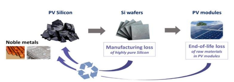
For solar cells, silicon purity often exceeds 99.9999% to achieve optimal efficiency and performance.
Silicon Purity Levels
Definition of Purity in Semiconductors
Purity in semiconductors refers to the concentration of intrinsic elements and the absence of foreign or extrinsic materials. In the context of silicon, a key component for semiconductor devices, purity is crucial because even trace amounts of impurities can dramatically affect the material’s electrical properties.
Measurement Methods
Different methods exist to measure the purity of silicon. High-Resolution Mass Spectrometry (HRMS) and Secondary Ion Mass Spectrometry (SIMS) are two primary methods used. HRMS measures the atomic mass and concentration of elements, providing detailed information on the elemental composition of the sample.
Impurity Impact
For silicon to function effectively as a semiconductor, its purity level needs to be extremely high, often 99.9999% or even higher. Impurities can introduce unwanted energy levels within the silicon’s bandgap, reducing its efficiency in converting light into electricity.
The Importance of Purity in Silicon-Based Solar Cells
The purity of silicon used in solar cells is directly tied to the cell’s performance. A solar cell’s primary function is to convert sunlight into electricity, and the efficiency of this conversion is heavily influenced by the purity of the silicon used.
Impact on Efficiency
Impurities in silicon can lead to electron-hole recombination. This recombination reduces the number of free electrons available to produce electricity, thereby decreasing the cell’s efficiency. For instance, a high purity monocrystalline silicon solar cell can reach efficiencies above 20%, while lower purity levels might reduce this to around 15% or even less.
Cost Implications
Higher purity silicon typically costs more to produce due to the stringent refinement processes required. While a higher initial cost may be involved, the return on investment over time can be greater due to the increased efficiency and longer lifespan of high-purity silicon solar cells. For example, a high-quality monocrystalline solar panel might have a lifespan of 25-30 years with minimal degradation in performance, justifying the higher upfront cost.
Size and Specifications
Solar panels made of higher purity silicon can potentially be smaller in size for the same power output, given their higher efficiency. This means that for a 300W panel, high purity silicon might require dimensions of 1.6m x 1m, whereas lower purity silicon might necessitate 1.8m x 1.2m, affecting installation and space considerations.
Quality and Longevity
The quality and longevity of a solar panel are directly influenced by the purity of the silicon used. Higher purity silicon can endure the stresses of temperature fluctuations and weather conditions better, leading to longer operational lifetimes and maintaining performance metrics over extended periods.
This detailed overview should help elucidate the importance of silicon purity levels, especially in the realm of solar cells.
Types of Silicon Used in Solar Cells
Monocrystalline Silicon
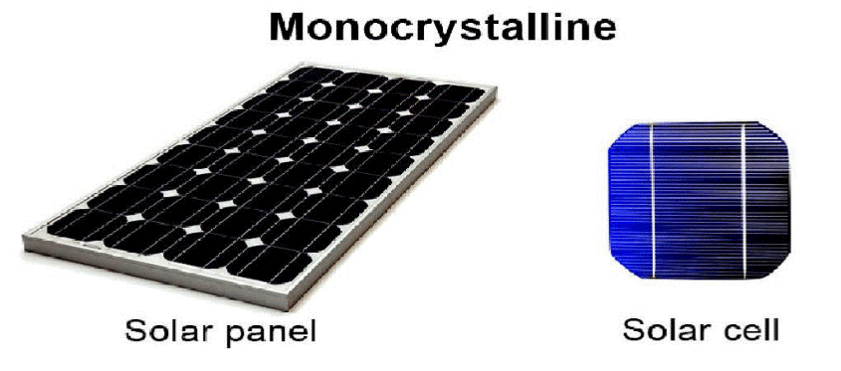
Monocrystalline silicon, often referred to as single-crystal silicon, is derived from a single, continuous crystal structure. It’s typically recognized by its dark black color and rounded edges.
Production Process
Manufacturers grow monocrystalline silicon in long cylindrical shapes, commonly using the Czochralski process. The process involves melting high-purity polysilicon and using a seed crystal to draw out a single crystal silicon ingot.
Efficiency and Cost
Due to its pure and uniform crystal structure, monocrystalline silicon offers higher efficiency, often exceeding 20%. However, this comes at a price, with monocrystalline panels typically being more expensive than their polycrystalline counterparts. An average monocrystalline solar panel might cost around $0.80 per watt, depending on the manufacturer and location.
Advantages and Disadvantages
The primary advantage of monocrystalline silicon is its high efficiency, which means installations require fewer panels for the same power output. This efficiency is particularly beneficial for space-constrained installations. On the flip side, the main disadvantage is the higher cost associated with its production.
Polycrystalline Silicon
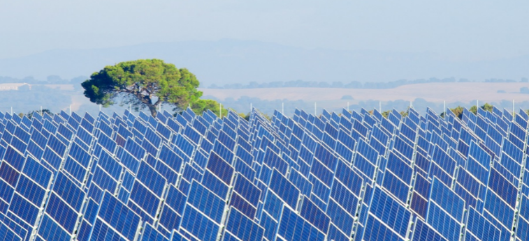
Polycrystalline silicon, also known as multi-crystalline silicon, consists of many small silicon crystals. It has a characteristic blue hue due to the way light interacts with the multiple crystals.
Production Process
The production of polycrystalline silicon is relatively straightforward. Manufacturers melt raw silicon and then allow it to cool and solidify in a mold, resulting in multiple crystals.
Efficiency and Cost
Polycrystalline silicon has an efficiency range between 15% to 18%. It is generally less expensive to produce than monocrystalline silicon, with prices for panels hovering around $0.70 per watt.
Advantages and Disadvantages
While polycrystalline panels come at a more affordable cost, their efficiency is typically lower than monocrystalline panels. This could mean a larger installation area is required for the same power output. However, the reduced production waste and cheaper price make it a preferred choice for large-scale installations with ample space.
Amorphous Silicon
Amorphous silicon differs from the other two types in that it doesn’t have a crystalline structure. Instead, the silicon atoms are arranged in a random fashion.
Production Process
Produced using a process called vapor deposition, a thin layer of amorphous silicon is deposited onto a substrate, often glass or another type of silicon.
Efficiency and Cost
Amorphous silicon solar cells have a relatively low efficiency, typically around 6% to 8%. They’re cheaper to produce than crystalline silicon cells, but their lower efficiency often necessitates more extensive installations for equivalent power outputs.
Advantages and Disadvantages
The primary advantage of amorphous silicon is its flexibility. Solar panels made from amorphous silicon can be thin and flexible, suitable for applications like solar-powered calculators or curved surfaces. The main drawback is its lower efficiency compared to crystalline forms of silicon.
This overview provides a comprehensive understanding of the types of silicon used in solar cells and their inherent properties, benefits, and challenges.
Methods for Achieving High Purity Silicon
The Tongwei Process
The Tongwei process is one of the most widely used methods for producing high-purity silicon, especially for the semiconductor industry.
Process Description
In the Tongwei process, highly purified trichlorosilane gas (HCl3Si) gets exposed to a heated silicon rod in a reactor. As the gas encounters the rod, it decomposes, and deposits additional silicon onto the rod. This deposited silicon has an extremely high level of purity.
Efficiency and Cost
The Tongwei process can achieve silicon purity levels exceeding 99.9999%. However, the process is energy-intensive, which can increase the cost. Typically, producing one kilogram of high-purity silicon through the Tongwei process consumes about 100-150 kWh of electricity.
Advantages and Disadvantages
The primary advantage of the Tongwei process is the exceptionally high purity levels it can attain. This high-purity silicon is vital for semiconductor applications where even trace impurities can affect performance. On the downside, the process’s energy intensity can result in higher production costs compared to other methods.
The Czochralski Process
The Czochralski process, while more associated with crystal growth, also plays a role in ensuring the silicon used is of high purity.
Process Description
The Czochralski process involves melting polycrystalline silicon in a crucible. A seed crystal, attached to a rod, is dipped into the melted silicon. The rod is then slowly pulled up and rotated, allowing a single crystal silicon ingot to form from the melt.
Efficiency and Cost
While the primary focus of the Czochralski process is to produce monocrystalline silicon structures, the process requires high-purity starting materials. As a result, the silicon produced often boasts purity levels comparable to those achieved by the Tongwei process. In terms of cost, the Czochralski method is also energy-intensive, with a single crystal growth consuming up to 60 kWh of electricity per kilogram of silicon.
Advantages and Disadvantages
The primary advantage is the production of large single-crystal ingots, which are ideal for high-efficiency solar cells and advanced semiconductor applications. However, the process does result in significant silicon waste, as the ingot’s outer parts are typically discarded to ensure uniformity and quality.
Other Refinement Methods
Several other methods exist for refining silicon, although they might not be as prevalent as the two mentioned above.
Zone Refining
Zone refining involves moving a molten zone through a silicon rod. As the molten zone moves, impurities get concentrated in the liquid region, leaving behind purer silicon.
Efficiency and Cost
Zone refining can achieve purity levels comparable to the Tongwei process. The cost can vary, but the process is generally less energy-intensive than the Tongwei or Czochralski methods.
Advantages and Disadvantages
Zone refining offers the advantage of less energy consumption and can be used to further refine silicon produced by other methods. The primary challenge is the scalability, as the process is more suited for small-scale operations.
This detailed insight into the methods for achieving high purity silicon highlights the intricacies and considerations involved in producing this vital material for the solar and semiconductor industries.
Effects of Silicon Impurities on Solar Cell Efficiency
Types of Impurities and Their Impact
Silicon impurities can originate from various sources, and even minuscule amounts can have a pronounced effect on the performance of a solar cell.
Metallic Impurities
Metallic elements such as iron, copper, and gold can get introduced into silicon during its production process. These metallic contaminants introduce deep energy levels in the silicon’s bandgap. For instance, iron, one of the most detrimental impurities, can drastically reduce the minority carrier lifetime, thereby decreasing the efficiency of a solar cell. The presence of just 10^13 atoms/cm^3 of iron can reduce a solar cell’s efficiency by up to 1%.
Oxygen and Carbon
Silicon wafers often contain oxygen and carbon due to the Czochralski process. While these impurities are not as harmful as metallic ones, they can still influence the electronic properties of the material. Oxygen, in particular, can lead to the formation of defects known as oxygen precipitates, which can impact the electrical performance.
Doping Materials
Though technically not impurities, doping agents like boron and phosphorus get introduced into silicon to modify its electrical properties intentionally. However, if concentrations are not controlled precisely, these doping materials can negatively affect the cell’s efficiency.
Measures to Minimize Impurities
Given the significant impact of impurities on solar cell efficiency, various measures are in place to minimize their presence.
Stringent Production Controls
Manufacturers have implemented rigorous controls in the production process to prevent contamination. This includes using high-purity raw materials, frequent testing, and maintaining cleanroom standards in facilities.
Gettering
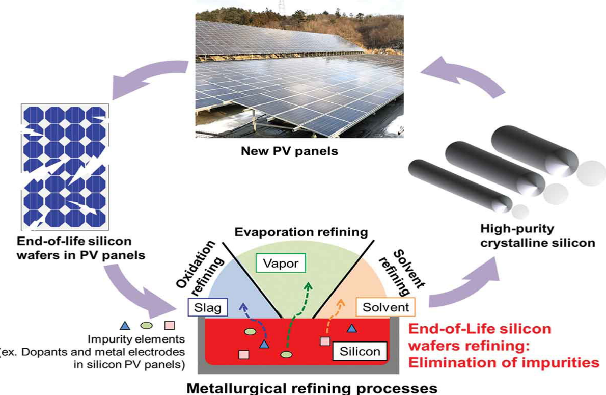
Gettering is a process where impurities in the silicon wafer get attracted to specific sites, effectively removing them from areas of the wafer that form the active part of the solar cell. For instance, phosphorus gettering can help remove harmful metallic impurities, improving the material’s quality and, in turn, the efficiency of the solar cell.
Advanced Refinement Techniques
Methods such as the Tongwei process and zone refining focus on producing the purest silicon possible. These processes achieve silicon purity levels exceeding 99.9999%, reducing the chances of impurities adversely affecting solar cell efficiency.
Quality Control and Testing
Regular testing of silicon wafers ensures that impurity levels remain within acceptable limits. Techniques such as Secondary Ion Mass Spectrometry (SIMS) enable the detection of even trace amounts of contaminants, ensuring that only the highest quality wafers move forward in the production process.
In conclusion, while silicon impurities can pose challenges to achieving optimal solar cell efficiency, ongoing advancements in production techniques, rigorous quality control, and refinement processes continue to mitigate these challenges.
Comparison with Other Materials
Silicon vs. Thin Film Technologies
Thin film technologies, such as cadmium telluride (CdTe) and copper indium gallium selenide (CIGS), present an alternative to traditional crystalline silicon solar cells.
Efficiency and Cost
While crystalline silicon panels commonly achieve efficiencies in the 18%-24% range, thin film technologies like CdTe typically hover around 11%-15%, and CIGS can reach up to 21% in laboratory conditions. However, the production cost for thin film technologies can be lower, with some manufacturers claiming costs as low as $0.50 per watt, compared to the average $0.70-$0.80 per watt for crystalline silicon.
Size and Flexibility
Thin film solar cells, as the name suggests, are much thinner than silicon wafers. This makes them flexible and suitable for applications like rollable solar panels or integration into building materials. Crystalline silicon panels, in contrast, are rigid and require robust mounting structures.
Lifespan and Degradation
Crystalline silicon panels boast lifespans exceeding 25 years with minimal degradation over time. Thin film panels, on the other hand, have shorter lifespans, often around 15-20 years, with faster degradation rates, especially in the initial years.
Silicon vs. Perovskite Solar Cells
Perovskite solar cells are a recent innovation, rapidly gaining attention due to their potential for high efficiency and low production costs.
Efficiency and Cost
While initial perovskite cells had modest efficiencies, recent developments have seen lab-tested cells achieve over 25% efficiency, rivaling and sometimes surpassing traditional silicon cells. Furthermore, the raw materials and production processes for perovskite cells can be significantly cheaper than silicon, though exact numbers can vary based on the specific technologies and methodologies used.
Production and Flexibility
Perovskite solar cells can be produced using solution-based processes, allowing for potential roll-to-roll manufacturing, similar to newspaper printing. This promises cheaper and faster production, and the resulting cells can be thin, lightweight, and flexible.
Stability and Longevity
While perovskite solar cells hold much promise, they currently face challenges in terms of stability and longevity. Exposure to moisture, heat, and UV radiation can degrade perovskite materials faster than silicon. Efforts are ongoing to enhance the stability of these cells and increase their operational lifespan.
In summary, while silicon remains the dominant material for solar cells, new technologies like thin film and perovskite cells present intriguing alternatives, each with its unique set of advantages and challenges. As research progresses and manufacturing techniques improve, the landscape of solar energy generation will continue to evolve.
Future Trends and Advancements
Towards Higher Purity Levels
The quest for ever-higher purity levels in silicon continues, driven by the relentless demand for enhanced efficiency and performance in both solar cells and electronic devices.
The Purity-Efficiency Relationship
With every increase in silicon purity, there’s potential to boost solar cell efficiency. For instance, achieving 99.99999% purity might push monocrystalline solar cell efficiencies beyond the 25% mark, resulting in more power generated from the same size and cost of the panel.
Implications for Electronics
Higher purity silicon also holds implications beyond solar cells. In the electronics industry, purer silicon can lead to faster and more efficient transistors, potentially revolutionizing the speed and performance of electronic devices.
New Technologies and Innovations in Silicon Refinement
Emerging technologies and innovations promise to reshape the landscape of silicon refinement, making the process more efficient, cost-effective, and environmentally friendly.
Plasma-Based Refinement
Plasma-based methods, which involve using ionized gases to refine silicon, promise to be less energy-intensive than traditional methods like the Tongwei process. These methods can potentially achieve high purity levels while consuming only a fraction of the energy.
Green Silicon Production
Environmental concerns are pushing the industry towards more sustainable silicon production methods. Techniques that use fewer chemicals, produce less waste, and consume less energy not only reduce the carbon footprint but can also lead to cost savings in the long run.
Integration with AI and Automation
The incorporation of Artificial Intelligence (AI) and automation in silicon refinement can lead to optimized processes, minimal human errors, and consistent quality. With AI-driven predictions, manufacturers can foresee and address potential impurities or defects in the silicon, ensuring higher quality and purity levels.
In conclusion, the future of silicon refinement is poised for transformation, with the twin goals of achieving unprecedented purity levels and making the refinement process more sustainable and efficient. These advancements will inevitably benefit industries ranging from renewable energy to electronics, reinforcing silicon’s pivotal role in modern technology.
